
Glass Coating Guide
What is glass coating?
Glass coating technology is a precision surface modification process based on the principles of surface engineering and thin-film optics. It involves depositing a functional layer—typically inorganic or organic-inorganic hybrid—ranging in thickness from nanometers to micrometers onto a glass substrate using methods such as physical or chemical vapor deposition (PVD/CVD), sol-gel processing, or magnetron sputtering. By forming a film layer with a specific microstructure on the substrate surface, this technology fundamentally alters the glass's surface energy, optical bandgap, and interfacial reaction characteristics, thereby imparting composite functionalities. In terms of optical performance, it leverages thin-film interference effects to achieve anti-reflective properties or selective spectral modulation (e.g., infrared reflection in Low-E coatings). Regarding surface characteristics, it constructs low-surface-energy hydrophobic/oleophobic layers that achieve water contact angles exceeding 90° or even surpassing 110°, enabling self-cleaning and easy-to-clean effects. In terms of mechanical properties, the coating enhances surface hardness and abrasion resistance while improving the glass's weatherability and chemical stability under complex environmental conditions.
Three Core Questions Before Selecting Coated Glass
The most critical aspect of your application lies in determining which challenge it primarily addresses: “optical” (transmission/reflection), “thermal” (insulation/heat dissipation), “electrical” (conductivity/electromagnetic shielding), or “surface” (easy-to-clean/anti-fingerprint).
Glass coating technology has never been a "one-size-fits-all" solution; it is more like a tool for making trade-offs across four dimensions: "optical, thermal, electrical, and surface." Different application scenarios have different pain points, leading to entirely different coating design philosophies. The following elaborates on these four dimensions.
If the focus is on "optical" – resolving the conflict between transmission and reflection. Typical scenarios include high-precision optical lenses and LiDAR windows. The core requirement in such applications is to "transmit the light that should be transmitted and reflect the light that shouldn't." Technically, this is often achieved using multi-layer dielectric films (e.g., alternating layers of titanium dioxide and silicon dioxide), leveraging the principle of light interference to drastically reduce the reflectivity of specific wavelengths (e.g., below 0.2%), achieving anti-reflection. Conversely, if the goal is to make glass reflective at certain angles while maintaining transparency from the other side, coatings can be used to achieve narrow-band filtering or dichroic reflection. The challenge in such applications lies in the extremely high precision required for film thickness and uniformity; even slight deviations can cause optical performance to fluctuate. Therefore, high-precision processes like ion-assisted deposition or magnetron sputtering are typically employed.
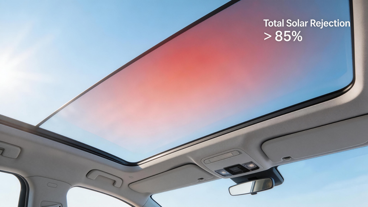
If the focus is on "thermal" – resolving the conflict between insulation and heat dissipation. Typical scenarios include energy-efficient architectural glass (Low-E) and new energy vehicle skylights. Triple-silver Low-E glass used in buildings involves coating glass with multiple layers of silver and dielectric materials, creating a "thermos" structure: it allows visible light to enter (maintaining brightness) while reflecting indoor infrared heat radiation back (for winter insulation) or blocking outdoor heat (for summer cooling). Ordinary glass has an emissivity of around 0.84, whereas triple-silver Low-E can achieve an emissivity below 0.02, resulting in vastly different thermal insulation effects. The challenge with automotive skylights is greater: they have large areas and curved shapes, requiring high thermal insulation efficiency (total solar energy rejection above 85%) without shielding signals like mobile phones, ETC, or 5G. Therefore, automotive applications often use nano-ceramic thermal insulation films (e.g., cesium tungsten bronze) or optimize silver-based film systems to balance insulation and signal transmission requirements.
If the focus is on "electrical" – resolving the conflict between conductivity and electromagnetic shielding.
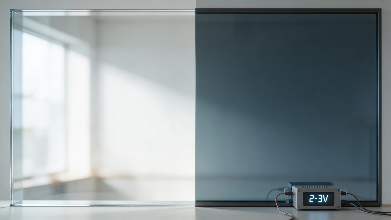
Typical scenarios include electrochromic smart windows, radomes, and electromagnetic shielding windows. The core material here is transparent conductive oxides, such as indium tin oxide (ITO). In electrochromic glass, the coating serves both as a conductive layer and as the "engine for color change": applying a small voltage (two to three volts) causes ions to insert into the electrochromic layer (e.g., tungsten trioxide), turning the glass from transparent to dark, and vice versa, enabling dynamic control of light and heat. Another scenario involves radomes or electromagnetic shielding windows for instruments, where the coating must block external electromagnetic interference (requiring extremely high conductivity) without affecting optical transmission. This is often achieved using metal mesh (copper or silver) or ultra-thin precious metal composite films, achieving very low sheet resistance while maintaining high light transmittance.
If the focus is on "surface" – resolving the conflict among easy cleaning, anti-fingerprint properties, and durability.
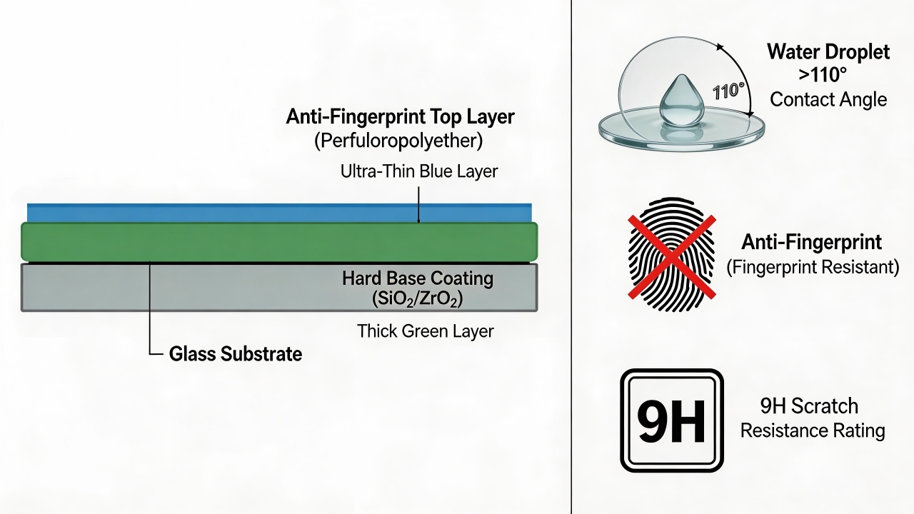
Typical scenarios include automotive cameras, mobile phone screens, and touch displays. The core idea is to alter the "character" of the glass surface—making it repel water, resist oil, and withstand abrasion. For automotive cameras, for example, an ultra-thin coating (a few nanometers thick) of fluorosilane or perfluoropolyether is applied, increasing the water contact angle from around 20-30 degrees on ordinary glass to over 110 degrees, creating a "lotus leaf effect." Raindrops bead up and roll off, and the airflow at high speeds easily clears them, ensuring a clear camera view. Mobile phone or automotive screens have even higher requirements: they need anti-fingerprint (AF) properties, scratch resistance (hardness enhancement), and a smooth tactile feel. Such solutions typically adopt a "hard base, soft surface" structure—a hard oxide layer (e.g., silicon dioxide, zirconium oxide) is first applied to increase the substrate's hardness, followed by a fluorinated anti-fingerprint layer. This achieves a pencil hardness of up to 9H with a low coefficient of friction, providing a smooth, durable, and pleasant user experience.
In summary, the four dimensions correspond to four distinct "core conflicts."
Optical: I need to transmit what should be transmitted and reflect what should be reflected, precisely controlling the spectrum.
Thermal: I need to manage heat, preserving it when necessary and insulating against it when necessary.
Electrical: I need both conductivity and transparency, or both electromagnetic shielding and optical clarity.
Surface: I need the glass to repel water, resist oil, withstand abrasion, and resist scratches.
In practical applications, many products represent a combination of multiple dimensions—for example, an automotive skylight needs thermal insulation (thermal), good light transmission (optical), no signal shielding (electrical), and durability against wear (surface). In such cases, coating design becomes a "systems engineering" challenge of finding a balance across these four dimensions.
What is the operating environment of your product: indoor, outdoor, extreme temperature zones, or chemical exposure?
For glass coatings used indoors—where they are not exposed to wind or rain but are touched, wiped, and rubbed repeatedly by fingers and cleaning cloths—typical examples include museum display cases, high-end monitors, and precision instrument windows. In such scenarios, the two biggest concerns are fingerprints and coating failure after frequent cleaning. Ordinary anti-fingerprint coatings, if they are just a thin fluorinated layer, can have their molecular chains break after a few thousand wipes with a non-woven cloth. The oleophobic properties degrade sharply, leaving the screen feeling rough and prone to smudges.
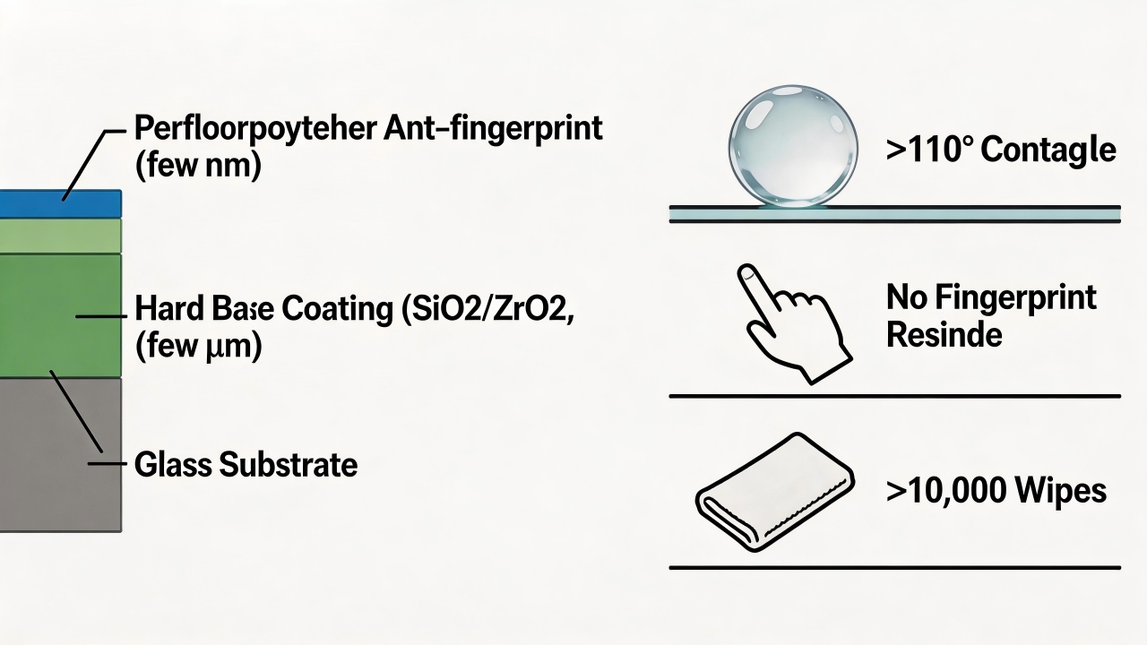
High-end indoor applications cannot simply borrow coatings designed for building exteriors. Instead, they adopt a "hard base, soft surface" approach: first, a hard underlayer a few micrometers thick, made of silicon dioxide or zirconium oxide, is applied to firmly anchor the substrate surface. On top of this, an extremely thin perfluoropolyether anti-fingerprint layer is deposited. This composite structure can increase the abrasion resistance from the usual three thousand wipes to over ten thousand, all without affecting optical clarity.
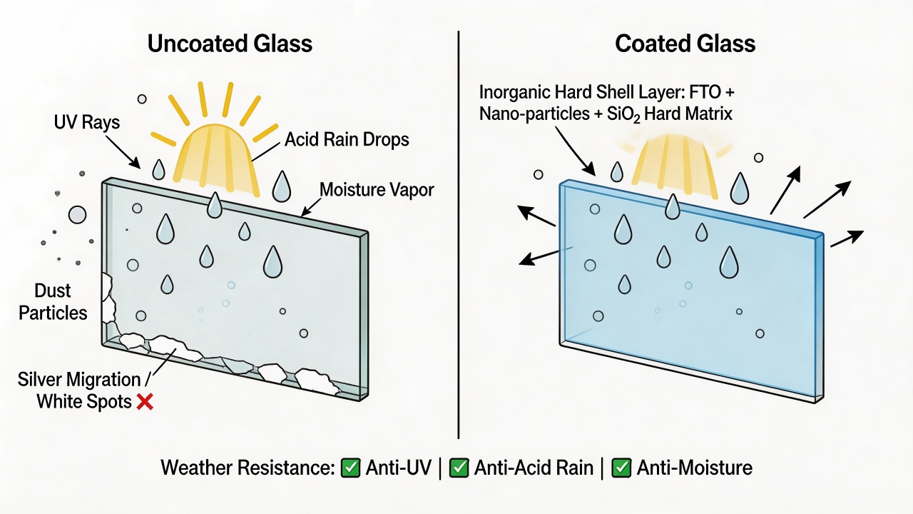
Outdoor environments are the ultimate test for coatings. Architectural façade Low-E glass, automotive skylights, and photovoltaic cover panels must simultaneously withstand solar radiation, temperature fluctuations, moisture ingress, acid rain, and dust. For Low-E glass, the critical silver layer is highly reactive. If moisture penetrates from the edge or if airborne sulfides exceed normal levels, the silver can migrate and agglomerate, forming white spots or black edges, which drastically reduces its infrared reflectivity. For automotive skylights, heat-insulating films are vulnerable to UV radiation; organic dyes or certain nano-ceramic materials can yellow over time, affecting appearance. The solution lies in an "inorganic hard protection" strategy: architectural glass can use fluorine-doped tin oxide applied directly at high temperatures—its optical performance is slightly inferior to off-line silver-based films, but its chemical stability is excellent, allowing it to resist outdoor acid and alkali corrosion. Automotive skylights encapsulate heat-insulating nanoparticles uniformly within an inorganic hard coating such as silicon dioxide, using a dense inorganic matrix to isolate oxygen and moisture, ensuring that the change in light transmittance remains within a very tight range even after thousands of hours of aging.
Extreme temperature zones represent another challenging scenario, such as aircraft windshields, polar building windows, high-temperature furnace observation windows, and new energy vehicle sensors. The core issue here is thermal expansion mismatch. In extreme cold, if the coating and glass contract at different rates, internal stress can build up to the point of cracking, potentially even weakening the glass itself. In extreme heat, ordinary organic coatings can carbonize directly, and even inorganic coatings may undergo phase transitions, causing volume changes that lead to peeling. For extreme cold, aircraft windshields often use a "graded interlayer" design—inserting a material with a coefficient of thermal expansion between that of the glass and the functional layer to gradually buffer the stress. For high-temperature observation windows, any organic material must be eliminated; pure inorganic hard coatings deposited by ion-assisted methods, such as certain transparent conductive films, can withstand temperatures above 500 °C without succumbing to thermal shock.
Finally, there are chemically aggressive environments: chemical plant control rooms, laboratory fume hoods, medical equipment touchscreens, and offshore wind turbine portholes. These places frequently come into contact with acids, alkalis, organic solvents, salt spray, and disinfectants. Conventional metal films (such as silver or copper) are highly susceptible to pinhole corrosion in salt spray or acidic gases—chloride ions penetrate through defects and cause electrochemical corrosion, leading to reduced transmittance and cosmetic damage. Polymer-based anti-fingerprint coatings can swell and peel when exposed to strong solvents like acetone or toluene. The solution is to use high-density, pinhole-free inorganic coatings. For example, chemical industry windows can be coated with diamond-like carbon or silicon nitride, which act as a dense chemical shield, effectively blocking moisture and ion migration. Medical equipment has even higher requirements: the coating must withstand repeated wiping with alcohol and hydrogen peroxide, as well as high‑temperature, high‑pressure steam sterilization (over 120 °C, saturated steam under pressure), without blistering or delamination. This often requires a thicker anti-fingerprint layer or a "fluorinated compound + silicon dioxide" composite structure to ensure reliability under extreme chemical conditions.
In summary:
Indoor coatings prioritize abrasion resistance and anti‑fingerprint performance—a "hard base, soft surface" approach.
Outdoor coatings prioritize weatherability and anti‑aging properties—an "inorganic hard shell" approach.
Extreme temperature zones require matching thermal expansion—a "graded interlayer" approach.
Chemically aggressive environments demand density and inertness—a "pinhole‑free barrier" approach.
Choosing the right coating starts with knowing where it will serve.
What is the operating environment of your product: indoor, outdoor, extreme temperature zones, or chemical exposure?
For glass coatings used indoors—where they are not exposed to wind or rain but are touched, wiped, and rubbed repeatedly by fingers and cleaning cloths—typical examples include museum display cases, high-end monitors, and precision instrument windows. In such scenarios, the two biggest concerns are fingerprints and coating failure after frequent cleaning. Ordinary anti‑fingerprint coatings, if they are just a thin fluorinated layer, can have their molecular chains break after a few thousand wipes with a non‑woven cloth. The oleophobic properties degrade sharply, leaving the screen feeling rough and prone to smudges.
High‑end indoor applications cannot simply borrow coatings designed for building exteriors. Instead, they adopt a “hard base, soft surface” approach: first, a hard underlayer a few micrometers thick, made of silicon dioxide or zirconium oxide, is applied to firmly anchor the substrate surface. On top of this, an extremely thin perfluoropolyether anti‑fingerprint layer is deposited. This composite structure can increase the abrasion resistance from the usual three thousand wipes to over ten thousand, all without affecting optical clarity.
Outdoor environments are the ultimate test for coatings. Architectural façade Low‑E glass, automotive skylights, and photovoltaic cover panels must simultaneously withstand solar radiation, temperature fluctuations, moisture ingress, acid rain, and dust. For Low‑E glass, the critical silver layer is highly reactive. If moisture penetrates from the edge or if airborne sulfides exceed normal levels, the silver can migrate and agglomerate, forming white spots or black edges, which drastically reduces its infrared reflectivity. For automotive skylights, heat‑insulating films are vulnerable to UV radiation; organic dyes or certain nano‑ceramic materials can yellow over time, affecting appearance. The solution lies in an “inorganic hard protection” strategy: architectural glass can use fluorine‑doped tin oxide applied directly at high temperatures—its optical performance is slightly inferior to off‑line silver‑based films, but its chemical stability is excellent, allowing it to resist outdoor acid and alkali corrosion. Automotive skylights encapsulate heat‑insulating nanoparticles uniformly within an inorganic hard coating such as silicon dioxide, using a dense inorganic matrix to isolate oxygen and moisture, ensuring that the change in light transmittance remains within a very tight range even after thousands of hours of aging.
Extreme temperature zones represent another challenging scenario, such as aircraft windshields, polar building windows, high‑temperature furnace observation windows, and new energy vehicle sensors. The core issue here is thermal expansion mismatch. In extreme cold, if the coating and glass contract at different rates, internal stress can build up to the point of cracking, potentially even weakening the glass itself. In extreme heat, ordinary organic coatings can carbonize directly, and even inorganic coatings may undergo phase transitions, causing volume changes that lead to peeling. For extreme cold, aircraft windshields often use a “graded interlayer” design—inserting a material with a coefficient of thermal expansion between that of the glass and the functional layer to gradually buffer the stress. For high‑temperature observation windows, any organic material must be eliminated; pure inorganic hard coatings deposited by ion‑assisted methods, such as certain transparent conductive films, can withstand temperatures above 500 °C without succumbing to thermal shock.
Finally, there are chemically aggressive environments: chemical plant control rooms, laboratory fume hoods, medical equipment touchscreens, and offshore wind turbine portholes. These places frequently come into contact with acids, alkalis, organic solvents, salt spray, and disinfectants. Conventional metal films (such as silver or copper) are highly susceptible to pinhole corrosion in salt spray or acidic gases—chloride ions penetrate through defects and cause electrochemical corrosion, leading to reduced transmittance and cosmetic damage. Polymer‑based anti‑fingerprint coatings can swell and peel when exposed to strong solvents like acetone or toluene. The solution is to use high‑density, pinhole‑free inorganic coatings. For example, chemical industry windows can be coated with diamond‑like carbon or silicon nitride, which act as a dense chemical shield, effectively blocking moisture and ion migration. Medical equipment has even higher requirements: the coating must withstand repeated wiping with alcohol and hydrogen peroxide, as well as high‑temperature, high‑pressure steam sterilization (over 120 °C, saturated steam under pressure), without blistering or delamination. This often requires a thicker anti‑fingerprint layer or a “fluorinated compound + silicon dioxide” composite structure to ensure reliability under extreme chemical conditions.
In summary:
Indoor coatings prioritize abrasion resistance and anti‑fingerprint performance—a “hard base, soft surface” approach.
Outdoor coatings prioritize weatherability and anti‑aging properties—an “inorganic hard shell” approach.
Extreme temperature zones require matching thermal expansion—a “graded interlayer” approach.
Chemically aggressive environments demand density and inertness—a “pinhole‑free barrier” approach.
Choosing the right coating starts with knowing where it will serve.
How to balance cost sensitivity and performance requirements?
In the aviation and optical fields, the balance between cost and performance for glass coatings follows a logic that is completely different from that of architectural glass—here, performance and reliability are always the top priorities, and cost sensitivity is relegated far behind. This is because, in these scenarios, coating failure can directly lead to system malfunction, mission failure, or even safety accidents, with consequences far outweighing the cost of the coating itself.
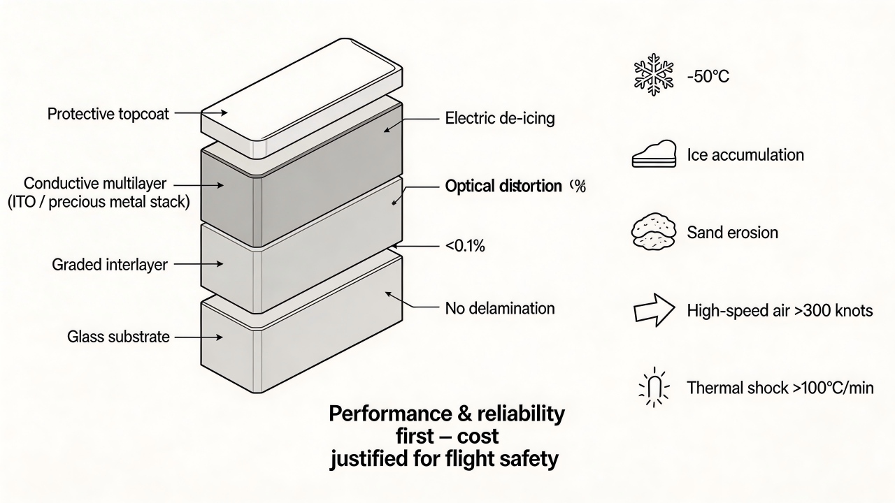
Take aircraft windshields as an example. The electrically heated coating (typically ITO or precious metal multilayer films) must meet extremely stringent requirements: rapid de‑icing in extreme cold as low as −50 °C, resistance to sand erosion at flight speeds exceeding 300 knots, survival under severe thermal shock (temperature changes >100 °C/min) without delamination, and an optical distortion rate for the pilot’s view kept below one‑thousandth. The process for such coatings is extremely complex—ion‑assisted deposition is used to ensure density, graded interlayers are added to eliminate thermal stress, and thickness uniformity must be controlled on curved substrates. The coating cost per unit can reach tens of thousands of yuan or even more, but this is a “necessary cost” for flight safety, leaving no room for compromise.
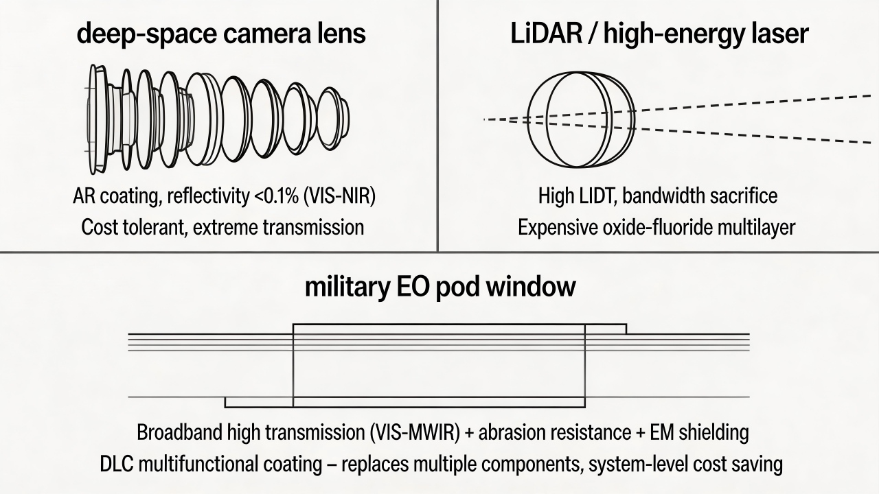
In the fields of precision optics and aerospace electro‑optical systems, the balance shifts toward “precise trade‑offs in performance specifications.” For example, anti‑reflection (AR) coatings for deep‑space exploration cameras or satellite optical windows pursue extreme transmission—reflectivity <0.1% in specific bands (such as visible to near‑infrared)—while being relatively tolerant of cost. However, for LiDAR or high‑energy laser systems, the coating must not only meet optical requirements but also possess an extremely high laser‑induced damage threshold (LIDT), which often means sacrificing some bandwidth or using more expensive oxide‑fluoride composite film systems. Another typical example is the window of military electro‑optical pods, which must simultaneously achieve broadband high transmission (visible to mid‑wave infrared), high mechanical strength, abrasion resistance, and electromagnetic shielding. This often leads to the use of diamond‑like carbon (DLC) or DLC‑based composite films. Although such films have slow deposition rates and narrow process windows, their “multi‑function in one film” capability replaces multiple discrete components, providing weight reduction and optical path simplification at the system level—a higher‑dimensional consideration of “cost‑effectiveness.”
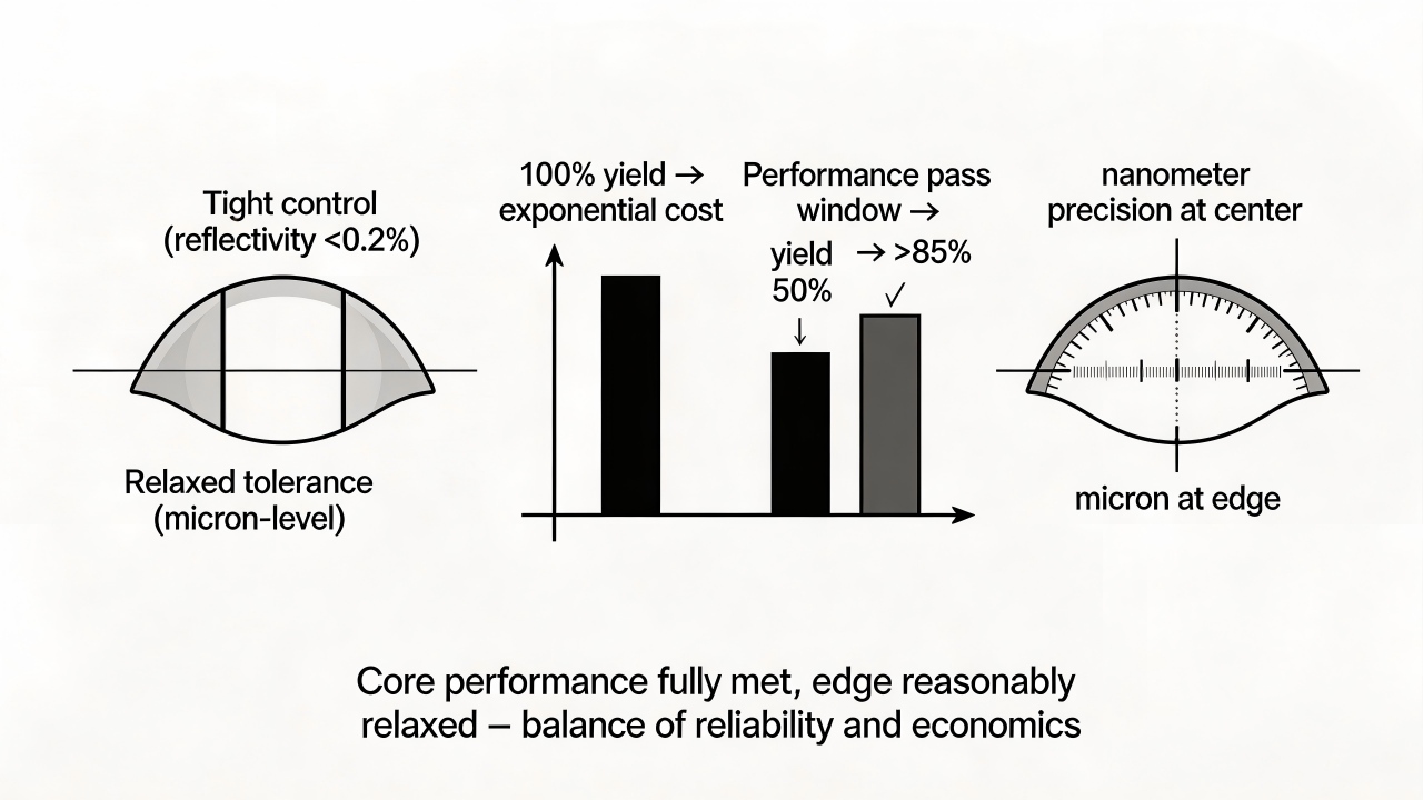
Furthermore, in high‑end optical lenses and spacecraft windows, cost balance is also reflected in the trade‑off between process yield and performance. For example, for aspherical or free‑form optical elements, controlling coating uniformity is extremely challenging. If a 100% yield is demanded, costs rise exponentially. Engineering practice often defines a “performance pass window”—allowing a very small edge region to have slightly higher reflectivity than the center, or granting micron‑level tolerances in film thickness—thereby increasing yield from 50% to over 85% while ensuring that the core optical performance fully meets mission requirements.
In summary, in the aviation and optical fields, balancing cost and performance is essentially a matter of treating the coating as a “critical system component” and applying reliability engineering management: aiming for “zero failure” by selecting mature processes and redundant designs, optimizing yield through precise performance grading (tight control in core areas, reasonable relaxation at edges), and evaluating at the system integration level the overall value brought by “multi‑function in one film.” The balance here is not “reducing performance to cut costs,” but rather pursuing the optimal solution of process feasibility and economic efficiency while ensuring absolute reliability.

Technical Objectives:
Complete Removal of Subsurface Damage: Ensuring the inherent strength and optical performance of the glass.
Achieving a Transparent Mirror Finish: Surface roughness reduced to Ra < 1 nm, with no visible scratches or haze to the naked eye.
Precise Figure Retention: Modifying the surface without compromising the geometric accuracy established during the grinding stage.
Key Parameters:
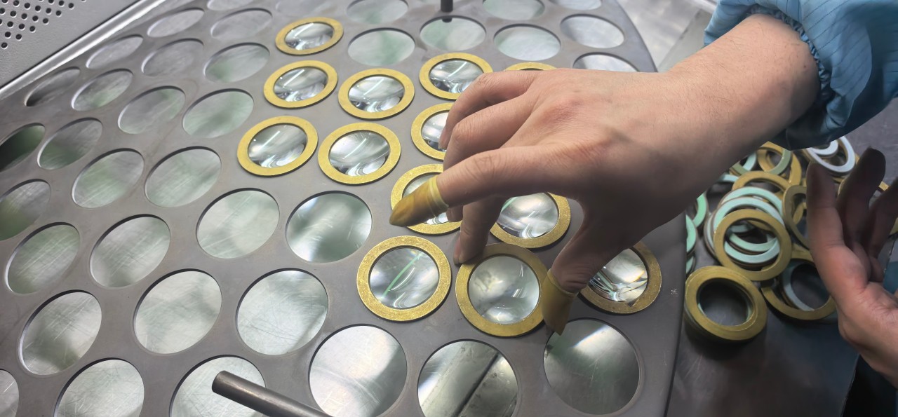
Abrasives: Cerium Oxide (CeO₂) – considered the "gold standard" for glass polishing, Zirconium Oxide (ZrO₂), Iron Oxide (Jeweler's Rouge).
Carrier/Polishing Pad: Polyurethane pads, pitch tools, felt cloth. Pitch polishing is the ultimate method for precision optical polishing.
Slurry pH Value, Concentration, Flow Rate; Temperature, Pressure.
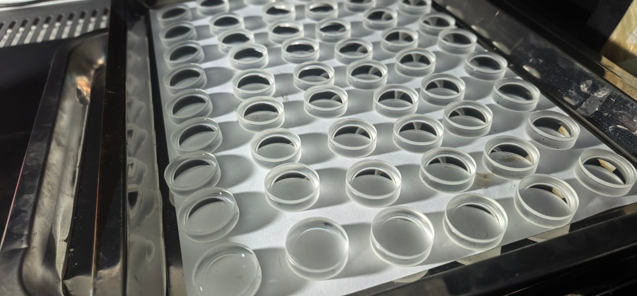
Typical Surface State:
Surface is completely transparent with a mirror-like reflection.
Roughness (Ra): 0.5 – 2.0 nm (for optical grades), potentially reaching atomic flatness (detectable by AFM).
No subsurface damage layer present (or damage depth less than 1/10 of the light wavelength).
Can the naked eye distinguish the difference between 99.5% and 99% transmittance? In what scenarios is it necessary to pursue the ultimate?
Under normal lighting conditions, the naked eye can hardly distinguish the difference between 99.5% and 99% transmittance.
1. Why can’t the naked eye tell the difference?
The human eye perceives brightness logarithmically, not linearly. According to the Weber-Fechner law, the just-noticeable difference in brightness is approximately 1%.
To put this in perspective:
99.5% transmittance means an incident light loss of 0.5%
99% transmittance means an incident light loss of 1%
The absolute brightness difference between the two is only 0.5%, which is far below the human eye’s perceptual threshold. In practice, even if two pieces of glass coated with 99% and 99.5% transmittance films are placed side by side under ordinary light sources, the vast majority of people cannot tell the difference. If the light source itself has slight fluctuations, if there are thickness tolerances in the glass, or if the viewing angle is slightly off, this difference is completely masked.
The point at which the naked eye can truly perceive a difference is usually below 98%—when transmittance drops from 98% to 95%, the human eye can just barely detect that the image is “a little darker.”
2. In what scenarios is it necessary to pursue the ultimate (99.5% or higher)?
Since the naked eye cannot tell the difference, why spend several times the cost to chase that extra 0.5%? The answer is: it’s not for the human eye, but for the system.
1. Weak light signal detection
In astronomical telescopes, deep-space exploration cameras, night vision devices, and single-photon detection systems, the incident light itself is extremely weak. For example, when a ground-based astronomical telescope observes faint celestial bodies, the number of photons reaching the sensor may be only a few dozen per second. In such cases, the transmittance loss of each optical element (lens, window, filter) directly reduces the signal-to-noise ratio.
A typical high-end astronomical camera optical path may contain 10–15 optical elements. If each element has 99% transmittance, the total system transmittance is approximately 86%; if each is improved to 99.5%, the total system transmittance reaches about 93%. This 7% system-level gain means nearly double the signal photons can be collected within the same exposure time—a critical factor for detection limits.

2. High-power laser systems
In scenarios such as laser cutting, LiDAR, and inertial confinement fusion (e.g., the National Ignition Facility), the coating is exposed to high-energy lasers. The logic for pursuing ultimate transmittance here is that every 1% of absorption or reflection translates into several watts to tens of watts of heat deposited into the coating at laser powers of hundreds or even thousands of watts.
Take a 1000 W continuous-wave laser as an example: 99% transmittance means 10 W is absorbed or reflected by the coating, which may cause thermal lensing (beam distortion), accelerated coating aging due to temperature rise, or even thermal damage. In contrast, 99.5% transmittance reduces the thermal load to 5 W, lowering the coating temperature by several tens of degrees Celsius and extending its lifetime several times over. In such applications, the 0.5% difference is the critical threshold for thermal management.
3. Multi-element optical systems
In precision optical systems such as high-end microscope objectives, lithography machine projection lenses, and zoom cinema lenses, the number of optical elements can reach 20–30. Taking the lens of a lithography machine as an example, its transmittance directly determines production line throughput.
As mentioned earlier, when multiple elements are stacked, a 0.5% difference per element is amplified into a 5%–10% difference at the system level. For a lithography machine that costs tens of millions or even hundreds of millions of yuan, every 0.1% increase in coating transmittance translates into several additional wafers processed per hour, with the annual output value increasing by millions of yuan. In this case, pursuing ultimate transmittance is an economic calculation, not a visual one.
4. Aviation and aerospace optical windows
In scenarios such as satellite optical payloads, airborne electro-optical pods, and astronaut extravehicular visors, the logic for pursuing ultimate transmittance is “system reliability margin.” After these devices are launched or deployed, there is almost no opportunity for repair. A coating with an initial transmittance of 99.5% may, after experiencing launch vibration, in-orbit ultraviolet radiation, and atomic oxygen erosion, still be above the design specification when its performance degrades to 99%. In contrast, a coating starting at 99% may fall below 98% after degradation, leading to reduced image quality at the end of the mission. In such scenarios, that 0.5% represents the lifetime margin.
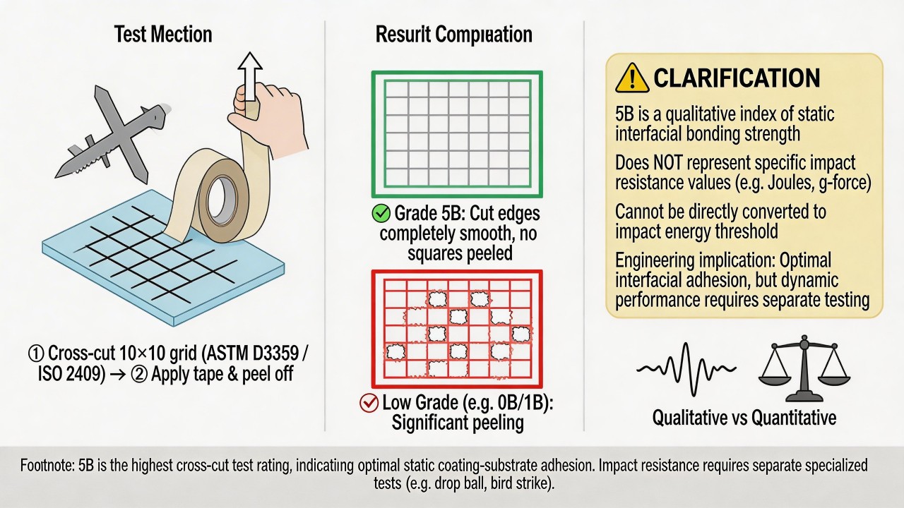
What mechanical impact resistance does an adhesion rating of 5B correspond to in practical use?
An adhesion rating of 5B is the highest level in cross‑cut testing (ASTM D3359 or ISO 2409), indicating that after cutting a 10×10 grid pattern in the coating with a cross‑cut tool and applying specialized tape for peeling, the edges of the cuts are completely smooth and no individual square has peeled off. This rating demonstrates that the static interfacial bonding strength between the coating and the substrate has reached an engineering “optimal” level. However, it is important to clarify that 5B itself does not correspond to a specific numerical value for mechanical impact resistance (such as a certain number of joules in a falling ball test or a certain peak acceleration in g). By nature, it is a qualitative indicator, not a quantitative parameter that can be directly converted into an impact energy threshold.
The reason 5B cannot be directly translated into an impact resistance value lies in the fundamentally different failure mechanisms between cross‑cut testing and mechanical impact testing. Cross‑cut testing evaluates the interfacial bonding strength of the coating under static shear and tensile conditions—the cutting tool creates micro‑cracks in the coating, and the peeling force applied by the tape is quasi‑static, reflecting the static strength of chemical bonds, van der Waals forces, or anchoring effects. Mechanical impact, on the other hand, involves dynamic energy absorption and multi‑axial stress coupling. When an impact occurs, the coating experiences multiple stresses simultaneously on a millisecond or even microsecond timescale: local compressive stress directly beneath the impact point, tensile bending stress around the impact point, shear stress at the coating‑substrate interface, and alternating loads from stress waves propagating within the material. A coating can pass the cross‑cut test perfectly (achieving 5B), but if it is too hard and lacks sufficient toughness, it may crack and delaminate under high‑speed impact because it cannot plastically deform with the substrate. Conversely, if the coating is too soft, it may be worn through by the impacting object without the adhesion itself failing. Therefore, 5B is a necessary condition for passing certain impact tests, but by no means a sufficient one—it ensures the coating “sticks,” but does not guarantee that it will “not crack, not fragment, or not detach” under dynamic loading.
In practical engineering applications, the relationship between 5B adhesion and mechanical impact resistance must be analyzed based on the coating material system, thickness, substrate type, and impact conditions. The following provides quantitative explanations according to different coating types and scenarios:
Category 1: Hard oxide/nitride coatings (e.g., SiO₂, TiO₂, Si₃N₄, DLC)
These coatings have high hardness (typically 5–30 GPa) and high elastic modulus, and are commonly used as protective or anti‑reflective layers on precision optical lenses, industrial windows, and aircraft windshields. With 5B adhesion, the mechanical impact resistance is primarily limited by the coating’s brittleness. In falling ball impact tests, for hard coatings with a thickness of 100–300 nm, they typically withstand a 130 g steel ball dropped from a height of 30–50 cm (impact energy approximately 0.4–0.65 J) without delamination, though micro‑cracks may appear around the impact point (radial cracks that do not propagate to the point of peeling). When the impact energy exceeds 0.8 J, even with 5B adhesion, the coating may undergo brittle delamination because the bending strain exceeds its fracture toughness (typically <3 MPa·m¹/²) due to local plastic deformation of the substrate. In sand‑dust erosion tests (MIL‑STD‑810 Method 510.8), 5B hard coatings typically withstand erosion at a sand concentration of 2.2 g/m³ and wind speed of 18 m/s for 60 minutes, with a mass loss rate <0.5%. However, after 90 minutes, even if adhesion remains intact, the coating may be worn through to expose the substrate due to cumulative abrasion.
Category 2: Metal or transparent conductive coatings (e.g., ITO, silver‑based multilayer films, Au/Pt)
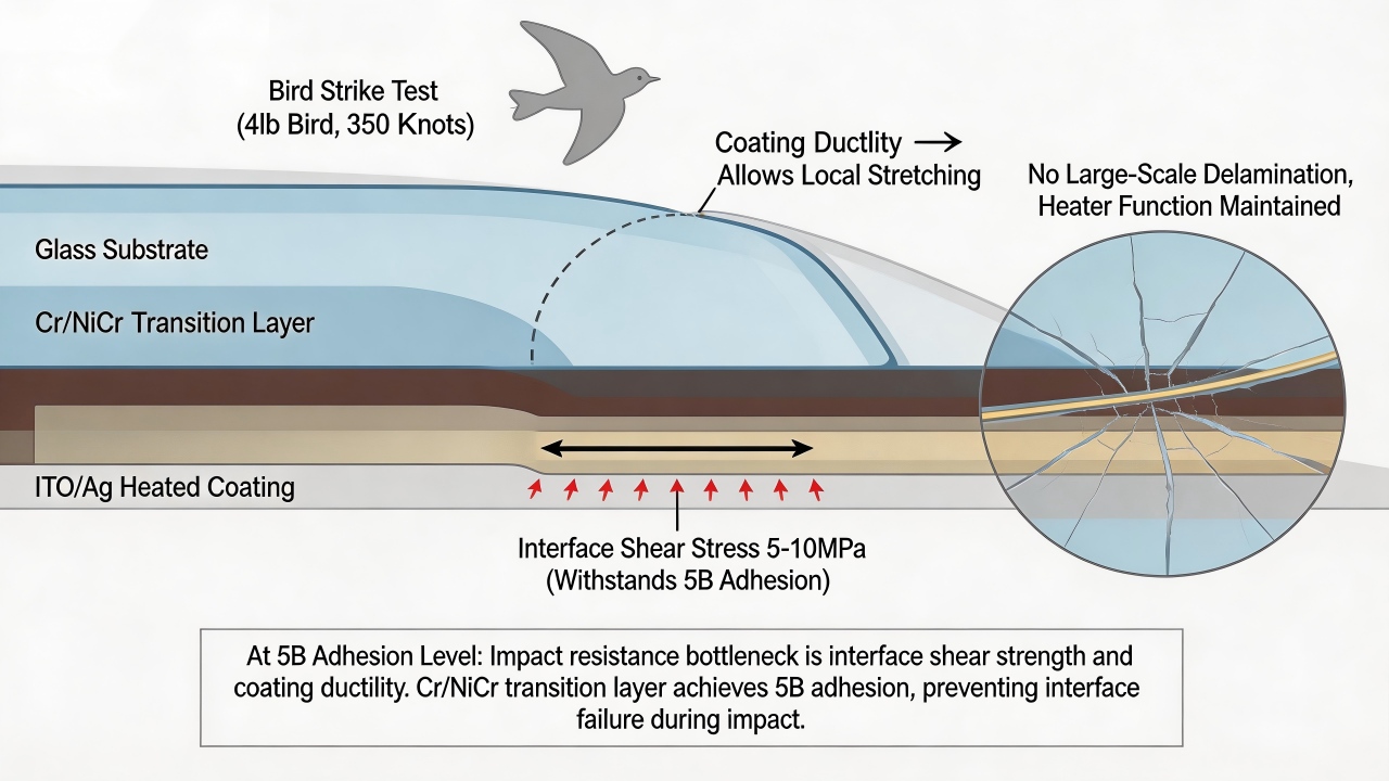
These coatings have relatively low hardness (ITO approximately 5–7 GPa, pure silver approximately 1–2 GPa) and better toughness, and are commonly used in aircraft windshield electric heating, automotive touch controls, and electromagnetic shielding windows. With 5B adhesion, the main bottlenecks for impact resistance are interfacial shear strength and coating ductility. Taking aircraft windshield electric heating films (ITO or Ag multilayer films, thickness approximately 150–500 nm) as an example, during bird strike tests (4‑lb bird, 350 knots), the windshield glass may fracture and experience bending deflections of several millimeters, but a 5B coating is required to maintain functionality without extensive delamination to ensure continuous electrical heating performance. This corresponds to withstanding a dynamic impact with a peak pressure of approximately 200–300 psi and duration <5 ms, with interfacial shear stresses reaching 5–10 MPa. In falling ball tests, such coatings are generally more “forgiving” than hard oxides—due to the plastic deformation capability of the metal layers, even if the substrate cracks, the coating can stretch locally along the crack edges without immediate delamination, typically withstanding impact energies of 1–1.5 J (130 g steel ball dropped from 80–120 cm), provided that a 5B adhesion level is achieved through the use of transition layers such as Cr or NiCr between the coating and the substrate.
Category 3: Organic or organic‑inorganic hybrid coatings (e.g., fluorosilane AF anti‑fingerprint coatings, polysilazane hard coatings)
These coatings have low hardness (typically <3 GPa) and low elastic modulus, and are commonly used on consumer electronics covers and automotive displays. With 5B adhesion, the mechanical impact resistance is primarily limited by the coating’s intrinsic strength and abrasion resistance. In Taber abrasion tests (CS‑10 wheels, 500 g load, 500 cycles), 5B adhesion ensures that the coating does not peel off in large areas during the wear process, but the organic layer itself may be worn through. In this case, although the adhesion remains at 5B, the functional layer has already failed. In falling ball tests, these coatings are relatively “soft” and can buffer some of the impact energy. When a 130 g steel ball is dropped from 30–50 cm, the coating typically remains intact. However, when the impact energy exceeds 0.8 J, even with 5B adhesion, the organic layer may locally lift due to cutting by sharp edges formed when the glass substrate fractures.
Category 4: Aerospace and specialty coatings (e.g., DLC, ITO+Si₃N₄ composite multilayer films)
These coatings often adopt multilayer composite structures (e.g., a Si₃N₄ protective layer deposited on an ITO conductive layer, further coated with a DLC wear‑resistant layer), with 5B adhesion required at each interface. Under such “redundant design,” impact resistance is significantly improved. Taking aerospace optical windows as an example, through the use of graded interlayers (e.g., a multilayer gradient structure of substrate/SiOₓ/Si₃N₄/ITO/DLC), after thermal cycling tests from −40 °C to +85 °C (10 cycles, temperature change rate >15 °C/min), the 5B adhesion is maintained, and the coating passes MIL‑STD‑810 Method 516.8 impact tests (40 g peak acceleration, 11 ms half‑sine wave) without any interfacial failure. The impact resistance of such composite coatings is 3–5 times that of single‑layer coatings, but the cost is correspondingly several times higher.
From an engineering practice perspective, the role of 5B adhesion in mechanical impact resistance can be summarized as “a threshold indicator, not an upper‑limit indicator.” It ensures that the coating possesses the fundamental interfacial bonding capability to withstand dynamic loads—if a coating does not even achieve 5B, early‑stage delamination under impact conditions is almost inevitable. However, once 5B is achieved, the specific impact energy, peak stress, or strain rate that the coating can withstand depends on its intrinsic properties (hardness, fracture toughness, elastic modulus) and coating system design (thickness, number of layers, interlayers, gradient structures).
For mission‑critical applications (aircraft windshields, automotive safety components, aerospace optics), the standard engineering approach is a three‑step validation: “5B adhesion + dedicated impact testing + failure mode analysis.” That is, adhesion is first ensured to reach 5B, then direct testing is conducted for the specific conditions (drop height, bird strike speed, vibration profile, sand‑dust concentration), rather than attempting to convert 5B into a theoretical impact threshold. At the same time, failure mode analysis is used to distinguish between “adhesion failure” (interfacial delamination) and “coating intrinsic failure” (cracking, wear‑through), thereby optimizing the coating system design—the former requires improved interface treatment (e.g., plasma cleaning, adding interlayers), while the latter requires adjusting the coating material or thickness.
In summary, the mechanical impact resistance of an adhesion rating of 5B in practical use is not a fixed value, but rather a range determined by four factors: “the 5B threshold + coating material properties + coating system structure + impact conditions.” In the consumer electronics sector, 5B coatings typically withstand falling ball impacts of 0.5–1 J. In automotive applications, dedicated testing is required for validation. In aviation, 5B is a foundational requirement for airworthiness certification, and the ultimate impact resistance is confirmed through full‑scale tests such as bird strikes, hail impacts, and sand‑dust erosion. If you have a specific coating system and application scenario (e.g., “an ITO film of XX thickness on XX substrate that needs to pass a falling ball test of XX joules”), I can help analyze whether 5B adhesion is sufficient under those conditions and whether improvements such as adding interlayers, adjusting film thickness, or adopting composite structures are needed to enhance impact resistance.
Does 1000 hours of salt spray testing equate to how long in outdoor use?
There is no fixed conversion factor between 1000 hours of salt spray testing and actual outdoor service time. The core reason lies in the fundamental difference in corrosion mechanisms: neutral salt spray testing (ASTM B117) creates a single corrosive environment characterized by "constant 5% NaCl solution, constant temperature of 35°C, and continuous spray." In contrast, real outdoor environments involve complex, coupled factors such as temperature and humidity cycles, UV radiation, rainfall washing, atmospheric pollutants, and wet‑dry alternation. Therefore, it is impossible to simply convert using a formula like "1 hour equals X days."
In practical engineering, the outdoor service life corresponding to 1000 hours of salt spray testing varies greatly depending on the environmental conditions. In coastal industrial areas (high salt spray combined with high pollution), due to the synergistic effect of chloride ions and acidic gases such as SO₂, 1000 hours roughly equates to 6–12 months of outdoor exposure. In coastal residential areas, where wet‑dry alternation and rainfall washing occur, it roughly equates to 1.5–3 years. In inland cities, where salt spray contributes minimally and corrosion comes mainly from rain and pollutants, the correlation between 1000 hours of salt spray testing and 5–10 years or even longer of outdoor service is weak. For desert or dry inland regions, salt spray test results have almost no reference value.
The true value of salt spray testing lies in "horizontal comparison" and "threshold validation," rather than "longitudinal life prediction." Within the same process system, a product that passes 1000 hours of testing is clearly superior in corrosion resistance to one that passes only 240 hours. Additionally, 1000 hours is a common "passing mark" in industries such as automotive, aerospace, and marine engineering—passing the test indicates that the coating possesses the fundamental capability to serve in environments with chloride ion attack. However, to evaluate actual outdoor service life, it is necessary to combine salt spray testing with other assessments such as UV aging, humidity‑heat cycling, and thermal shock testing. If your application scenario involves coastal buildings or marine equipment, it is recommended to supplement salt spray testing with cyclic corrosion testing (CCT)—which alternates between salt spray, drying, and humidity‑heat conditions—as this method has a much higher correlation with real outdoor environments than constant salt spray testing.
Yield traps in vacuum coating: Which designs cause a sharp drop in yield?
In coating production, the shape of the substrate and the complexity of the coating system design are often the most insidious killers of yield. The following categories of situations are enough to give process engineers a headache.
1. Extreme aspect ratio and deep‑cavity structures
When the substrate is very small and very thin, or has deep holes, blind vias, or steep sidewalls, coating uniformity becomes extremely poor. Typical examples are AR glasses lenses or micro‑lens arrays, where the radius of curvature is only a few millimeters, yet the film thickness must be controlled within ±1 nm.
The problem lies in the coating principle: materials in magnetron sputtering basically travel in straight lines and deposit accordingly. When encountering a deep‑cavity structure, the amount of material that reaches the sidewall versus the bottom differs greatly, and the thickness difference can reach 30%–50%. An anti‑reflection coating originally designed for a wavelength of 550 nm (green light) may shift to above 600 nm on the sidewall, causing the reflectivity to jump from 0.5% to 3%–5%—the optical performance is completely ruined.
To improve uniformity, complex rotating fixtures, tilted deposition, and longer coating times are needed. Yet even then, the per‑batch yield is typically only 50%–70%, and the coating time per piece increases by a factor of two or three.
2. Coupling of large size and thin substrates
In architectural glass or automotive skylights, glass that is over 3 m long and 2 m wide yet only 2–3 mm thick is a "disaster zone" for yield.
Two main issues exist. The first is thermal‑stress warpage. During magnetron sputtering, the glass is heated to 150–250 °C. Such large, thin glass warps like a roof tile after heating and cooling, with bowing exceeding 5 mm per meter. After warping, the glass may hit the mask or transport rollers, causing scratches, or develop micro‑cracks in stress‑concentrated areas. The second issue is transport stability. In continuous production lines, oversized glass is transported by rollers. If warpage is excessive, the roller contact points leave periodic thickness non‑uniformities on the coating; in severe cases, the entire piece is scrapped.
Taking a 3.2 m × 1.8 m automotive skylight as an example, from the first piece to stable mass production, yield ramp‑up often takes 3–6 months. Even after stabilization, the yield is only 75%–85%, whereas conventional sizes easily exceed 95%.
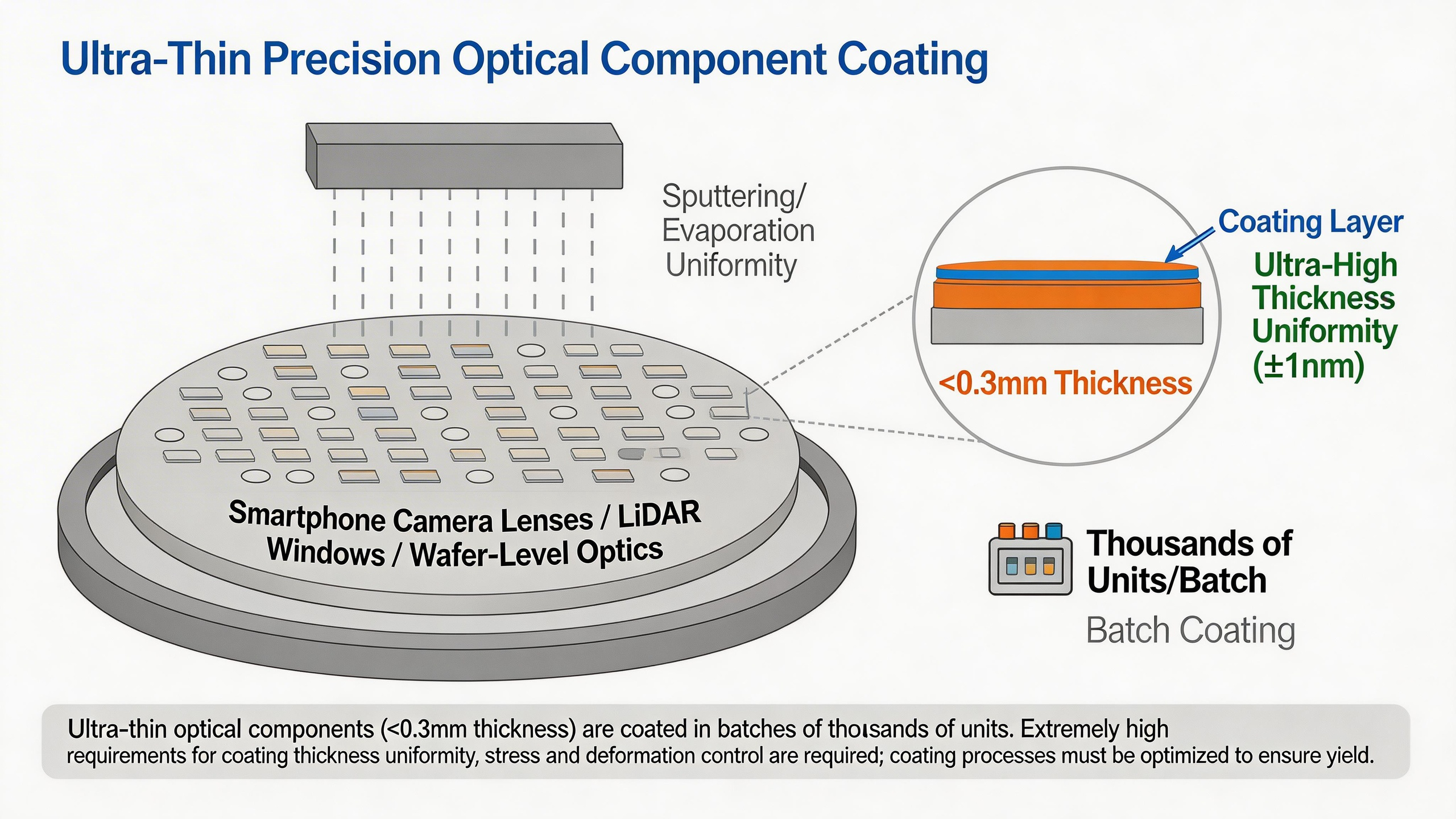
3. Ultra‑thin precision optical components
Smartphone camera lenses, LiDAR windows, and wafer‑level optics are often less than 0.3 mm thick, and thousands of pieces are coated in a single batch.
Three hidden killers exist here:
Edge effect: On planetary rotating fixtures, the film thickness on lenses at the edge of the tray can differ by 5%–8% from those at the center. For narrow‑band filters, which are extremely wavelength‑sensitive, a center‑wavelength shift of 2–3 nm causes functional failure.
Shadowing: The lenses are only a few millimeters in size. If the fixture’s clamping point is too close to the optical area, it creates a shadow on the coating—a graded peeling zone of 10–50 µm around the clamping point—which leads to uncontrolled stray light during lens assembly.
Electrostatic attraction: Ultra‑thin parts easily become charged in the vacuum chamber and attract dust. A single 5‑µm particle can scrap an entire lens.
The yield for such products is highly dependent on fixture design and cleanliness control. The industry average is between 75% and 90%. However, if the design does not clearly separate the optical area from the clamping area, the yield can drop directly to 40%–60%, with defects mainly being edge peeling, non‑uniform thickness, and particle contamination.
4. Multilayer complex coating systems and interlayer matching
When the number of coating layers exceeds 10, or when oxides are deposited directly on top of metal layers (e.g., silver, copper), the "compatibility" between layers becomes the key to yield.
A typical example is triple‑silver Low‑E glass, with a sandwich‑like structure: dielectric / silver / barrier / dielectric / silver / barrier / dielectric / silver / dielectric—more than ten layers.
Three major risks exist:
Interface oxidation: Silver is very reactive. If the barrier layer above it (usually NiCr alloy) is insufficient in thickness or poorly controlled, the silver can oxidize during subsequent coating processes, forming nano‑scale silver island agglomerates. This change may not be detected by adhesion testing, but the infrared reflectivity drops significantly, and the thermal insulation performance fails to meet specifications.
Stress accumulation: Each layer has internal stress (some tensile, some compressive). Beyond 10 layers, the total stress can reach several hundred megapascals. If the design does not achieve "stress balancing"—for example, using compressive layers to offset tensile layers—the coating system may spontaneously crack or peel entirely during temperature changes or cutting. Such failures often appear only after the final product is cut or tempered, resulting in substantial losses.
Vacuum environment conflicts: A complex coating system means the substrate must pass back and forth through multiple coating chambers many times. If the vacuum level in any chamber fluctuates due to maintenance cycles, residual water vapor becomes embedded in the growing film, forming pinholes or inter‑columnar voids that later become pathways for corrosive media.
Even on world‑class production lines, the mass‑production yield of triple‑silver Low‑E glass typically hovers between 80% and 90%. If the design neglects barrier‑layer thickness redundancy or stress‑matching calculations, the initial yield may be only 50%–60%, with failures mainly showing as "performance non‑compliance" and "edge chipping after tempering," often requiring several months of tuning to ramp up.
Limitations of different processes on substrate size and shape
Different coating processes have distinct constraints on substrate size and shape, and these constraints often directly determine whether a product design can be mass‑produced. The typical limitations of the mainstream processes are as follows.
1. Magnetron sputtering
Magnetron sputtering has clear upper and lower limits on substrate size. In architectural glass applications, continuous sputtering lines can handle oversized glass up to 3.3 m wide and 6 m long or even larger—this is one of the core advantages of this process. However, when the substrate is too small (e.g., less than 50 mm × 50 mm), fixturing, transport, and uniformity control become difficult, and the per‑batch yield drops significantly. In terms of shape, magnetron sputtering is essentially a line‑of‑sight deposition process—target atoms travel to the substrate in nearly straight lines. This means that flat or nearly flat substrates (radius of curvature >500 mm) are most suitable. For deep cavities, steep sidewalls, or complex shapes with a small radius of curvature (e.g., <50 mm), the thickness difference between sidewalls and bottom can reach 30%–50%, and shadowing effects are pronounced. Although rotating fixtures, tilted deposition, and other measures can partially improve the situation, they significantly increase process complexity and cycle time, and are generally only suitable for small‑batch specialty needs.
2. Vacuum evaporation
Vacuum evaporation imposes relatively loose constraints on substrate size and can be used both for large architectural glass (electron‑beam evaporation) and for miniature optical components. However, the core limitation lies in the distribution characteristics of the evaporation source—the evaporation intensity from a point source or area source varies dramatically with angle and distance. For large‑area substrates, rotating planetary fixtures or source scanning must be used to ensure uniformity, which limits the loading density and cycle time per batch. In terms of shape adaptability, evaporation, like sputtering, is a line‑of‑sight process and has weak coverage for deep holes, sidewalls, and complex curved surfaces. Nevertheless, evaporation has a unique advantage: it can achieve patterned coatings through tilted evaporation or shadow masking, which is irreplaceable in optical filter and MEMS device manufacturing. The disadvantage is that the adhesion of evaporated films is usually weaker than that of sputtered films, so caution is needed for applications requiring mechanical stress resistance.
3. Sol‑gel
The sol‑gel process offers the greatest flexibility in terms of substrate size and shape. Dip coating can handle everything from millimeter‑scale lenses to meter‑long tubes, as long as the substrate can be immersed in the sol bath. Spin coating is suitable for wafer‑scale or flat‑panel substrates, typically limited to sizes up to 12 inches. Spray coating has virtually no upper size limit and can cover large‑area applications such as architectural curtain walls and photovoltaic glass; it also adapts extremely well to curved or irregularly shaped parts—in theory, any shape that can be reached by the spray nozzle can be coated. However, the price of sol‑gel is that for large sizes or complex shapes, thickness uniformity control is far inferior to that of vacuum coating; performance often has to be sacrificed in edge areas to meet specifications in the center. In addition, the thermal treatment step requires the substrate to withstand baking temperatures of 100–500 °C, so heat‑sensitive materials (e.g., certain plastics, organic substrates) are not suitable.
4. Plasma‑enhanced chemical vapor deposition (PECVD)
PECVD is mainly used to prepare silicon‑based dielectric films (e.g., Si₃N₄, SiO₂) and diamond‑like carbon (DLC) films. In terms of size, PECVD is limited by the volume of the vacuum chamber and the electrode configuration. Common planar PECVD systems can handle glass substrates from G4.5 (approximately 1.2 m × 0.9 m) up to G8.5 (approximately 2.5 m × 2.2 m) for TFT‑LCD or photovoltaic applications. Tubular or barrel PECVD systems are more suitable for small‑size wafers or batch processing of discrete parts. Regarding shape adaptability, PECVD offers significantly better conformal coverage of complex three‑dimensional shapes than sputtering or evaporation—because the reactive species in the plasma diffuse isotropically, uniform films can be deposited inside micron‑scale trenches, sidewalls, and even through‑holes. This is the reason for its widespread use in the semiconductor and MEMS fields. However, for macroscopic curved surfaces (e.g., automotive skylights), PECVD is still mainly applied to nearly flat substrates, because maintaining a large‑area uniform plasma is itself challenging.
5. Atomic layer deposition (ALD)
Atomic layer deposition is the most shape‑adaptable technology, bar none. Through self‑limiting surface reactions, ALD can achieve atomically uniform conformal coverage on the surfaces of high‑aspect‑ratio (>100:1) deep holes, complex three‑dimensional structures, and powder particles. In terms of size, ALD is limited by the volume of the reaction chamber. Current commercial equipment typically handles substrates up to G4.5 (approximately 1.2 m × 0.9 m); larger sizes involve extremely high equipment costs and slow cycle times. Therefore, ALD is mainly used for high‑value‑added small precision devices such as optical lenses, MEMS sensors, semiconductor devices, and OLED encapsulation, rather than for large‑area architectural or automotive glass.
Delamination: Is it an adhesion problem or a substrate cleaning problem?
Delamination—the peeling of a coating from its substrate—essentially has only two root causes: either the substrate was not cleaned properly, or the substrate was clean but the coating and substrate are "incompatible." The former is like tiling a dirty wall: the tiles are actually sticking to dust or grease, and they fall off in whole pieces with a light touch. The latter is like having a clean wall but using the wrong cement mix or having mismatched thermal expansion—over time or with temperature changes, the tiles still lift off. Accurately distinguishing between these two causes is the first step in solving delamination problems.
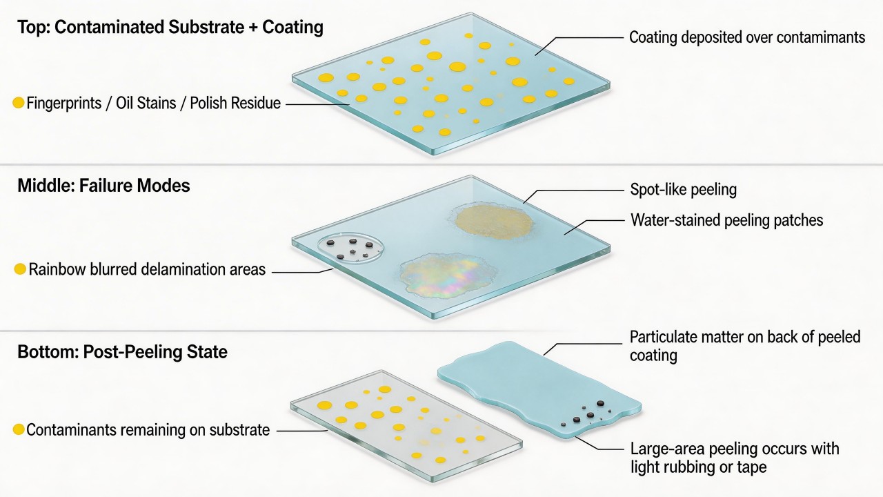
If contaminants are present on the substrate surface (fingerprints, oil stains, cleaning agent residues, polishing compounds, airborne silicones, etc.), the deposited coating actually sits on top of the contaminants rather than on the substrate itself. The contaminants act as a weak interfacial layer that fails first when stressed. The characteristic features of this type of delamination are random, patternless distribution—appearing as spots, fingerprints, water stains, or even rainbow patterns or hazy patches. After peeling, the substrate surface often still has residual contamination, or the backside of the coating carries adhered particles. Problems typically appear quickly; light wiping or tape peeling causes large‑area detachment. Solutions include optimizing cleaning processes, adding plasma pretreatment, and strictly controlling handling and storage environments.
If the substrate cleanliness meets standards but the intrinsic adhesion strength between the coating and substrate is insufficient, delamination arises from physical or chemical mismatches. Examples include: the substrate surface energy is too low for the coating material to wet and spread; the thermal expansion coefficients of the coating and substrate differ too much, generating high stress during thermal cycling; or the internal stress within the coating is so high that it cracks itself apart. The characteristic features of this type of delamination are patterned and regular—whole‑sheet peeling, propagation from edges inward, or preferential failure in specific patterned areas. After peeling, the substrate is clean with no residues, and the backside of the coating is smooth. Problems may appear immediately after coating or may develop gradually after thermal shock, mechanical stress, or long‑term aging. Solutions include introducing graded interlayers, optimizing coating design to balance stress, selecting materials with better thermal expansion matching, and adding interfacial activation treatments.
In actual production, the two types of problems often coexist and interact. If contaminants are not thoroughly removed, even a coating with strong intrinsic adhesion will fail at the weak interfacial layer. If the substrate is clean but adhesion is weak, delamination will occur once environmental stresses build up. Making matters more complicated, residual contaminants can induce interfacial chemical reactions in humid or hot environments, accelerating adhesion degradation. Therefore, the correct troubleshooting sequence is: first, use contact angle measurements, XPS, or energy‑dispersive spectroscopy to confirm whether the substrate is truly clean. After ruling out contaminants, then analyze adhesion‑related factors such as stress matching, interface design, and process parameters. Only by precisely determining whether the problem is "didn't stick to the real thing" or "the real thing won't stick" can you avoid repeatedly adjusting processes without addressing the root cause.
Automotive interior touchscreen: glove touch, high‑temperature exposure, long‑term fingerprints – which lasts longer, the conductive coating or the oleophobic layer?
On automotive interior touchscreens, the lifespans of the oleophobic layer (anti‑fingerprint) and the conductive coating (ITO or metal mesh responsible for touch sensing) are not synchronized. Typically, the oleophobic layer fails first, but the conductive coating is by no means worry‑free. Their failure modes are completely different: the oleophobic layer gradually wears out and its performance degrades – the user can clearly feel this. The conductive coating, on the other hand, works fine until it doesn't, and when it fails, the result is touch malfunction, which is far more serious.
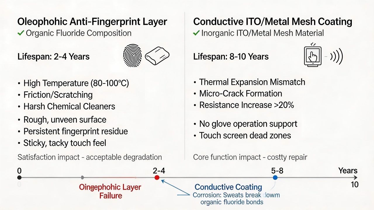
The reason the oleophobic layer has a short life in a car interior is the combined assault of high temperature and frequent use. Under summer sun exposure, the dashboard temperature can reach 80–100 °C. The oleophobic layer is essentially an organic fluoride compound; prolonged heating causes it to slowly degrade, so its anti‑fingerprint performance declines year by year. Add to that countless daily finger swipes and wiping clean – this nanoscale film is consumed by both physical abrasion and chemical corrosion from skin oils. Typically after 2–4 years, the oleophobic layer becomes noticeably "rough," fingerprints stick and are hard to wipe off, and the user first experiences a decline in satisfaction. In contrast, the conductive coating is an inorganic material (such as ITO or metal mesh) with a much longer intrinsic life, theoretically lasting 8–10 years or more.
However, the failure of the conductive coating is more insidious and more dangerous. It is not afraid of "heavy use," but rather of "being damaged by heat" or "being cracked by interfacial stress." Under prolonged high‑temperature exposure, the thermal expansion mismatch between the conductive film and the glass substrate accumulates stress, which can lead to micro‑cracks or even local delamination of the film, manifesting as reduced touch sensitivity in a certain area. Additionally, when operating with gloves, the glove increases the contact resistance, requiring the conductive layer itself to have sufficiently low resistance. If the resistance of the conductive layer rises by more than 20% due to oxidation or micro‑cracks, a progressive failure may appear – "can't respond when wearing thick gloves in winter." Such problems typically occur at a vehicle age of 5–8 years, later than the failure of the oleophobic layer, but once it happens, the repair cost is far higher than recoating an oleophobic layer.
Interestingly, the two layers can also "mask" each other's problems. After the oleophobic layer fails first, the user only notices that the screen feels sticky with fingerprints and is hard to clean, but touch still works – many people tolerate it and don't seek repair. However, once the oleophobic layer is gone, the salts and oils from fingerprints attach directly to the surface of the conductive coating. Long‑term accumulation can corrode the conductive layer (especially silver‑based metal mesh), indirectly shortening the actual life of the conductive coating. Therefore, the oleophobic layer affects "user experience satisfaction," while the conductive coating affects "functional reliability" – the latter directly relates to core operations such as climate control, entertainment, and drive mode selection.
From an automotive design perspective, engineers have different requirements for the two: the oleophobic layer is treated as a "consumable with acceptable degradation," generally required to last 3–4 years of normal use. The conductive coating, however, must ensure reliability for more than 10 years, because it is a core functional layer that cannot be allowed to fail easily. Thus, the user perceives the oleophobic layer as "the first to fail," but engineering efforts are truly focused on preventing early failure of the conductive coating. In summary: the oleophobic layer reaches the end of its life first, but does not affect functionality; the conductive coating fails later, but when it fails, it is a major problem.
Medical devices: disinfectant corrosion, autoclaving – which coatings can withstand the challenge?
In the medical device field, coatings face far harsher challenges than those in consumer electronics or automotive interiors – disinfectant corrosion and autoclaving form a dual "screening threshold." Coatings that can withstand both must simultaneously possess extremely high chemical inertness, a dense microstructure, excellent wet‑heat adhesion, and thermal stability matched to the substrate. Among the various coating systems, diamond‑like carbon (DLC) coating is widely recognized as an "all‑round performer" in the medical device field, particularly suitable for high‑contact surgical instruments on metal or ceramic substrates that require corrosion resistance, wear resistance, and low friction simultaneously. DLC coatings consist of sp² and sp³ hybridized carbon atoms, offering extremely high chemical inertness – they are essentially non‑reactive with most disinfectants including hydrogen peroxide, sodium hypochlorite, alcohol, and quaternary ammonium compounds. Their dense amorphous structure effectively blocks the penetration of moisture and chloride ions, preventing substrate corrosion. During autoclaving (typically 121 °C saturated steam, 0.2 MPa pressure, 20‑30 minute cycles), the greatest challenge for DLC coatings is adhesion. However, with the use of doped metal (e.g., titanium, chromium) interlayer designs, strong bonding to substrates such as stainless steel and titanium alloys can be achieved, withstanding hundreds of sterilization cycles without delamination. As a result, high‑quality DLC coatings can endure 100–200 autoclave cycles without peeling or performance degradation, and are widely used on high‑frequency surgical instruments such as scissors, orthopedic drills, and laparoscopic tools.
Silicon nitride and silicon oxide‑based hard coatings are another proven and reliable choice. Silicon nitride and silicon oxide are inorganic ceramic coatings deposited by PECVD or magnetron sputtering, and are widely used in medical devices, laboratory ware, and microfluidic chips. Silicon nitride offers extremely high chemical stability, resisting acids, alkalis, and oxidizing disinfectants such as peracetic acid and chlorine‑based disinfectants. Its very low water vapor transmission rate effectively protects glass or metal substrates from corrosion. Under autoclave conditions, the thermal stability of silicon nitride (decomposition temperature >1800 °C) far exceeds sterilization temperatures, and its coefficient of thermal expansion (approximately 2.5–3.5 ppm/°C) matches well with substrates such as glass and silicon, allowing it to withstand severe temperature changes without cracking. Silicon oxide coatings focus more on "sacrificial protection" – a dense SiO₂ layer blocks corrosive media. Although slightly less hard than silicon nitride, silicon oxide offers better biocompatibility and relatively lower cost. In practice, silicon nitride coatings on glass substrates can withstand more than 500 autoclave cycles, while optimized silicon oxide coatings can endure 200–300 cycles, mainly used on glass or quartz laboratory reactors, microfluidic chips, and endoscopic optical windows.
Specific metal and noble metal coatings become necessary for medical devices requiring conductivity, antimicrobial properties, or X‑ray visibility. Titanium and its nitrides (TiN, TiCN) are the most widely used metal coatings in medical devices – titanium naturally forms a dense, passivated oxide film that is highly resistant to chloride ions, hydrogen peroxide, and other corrosive media. TiN coatings are hard, chemically inert, and have a distinctive gold color for easy instrument identification. Noble metal coatings such as platinum, iridium, and gold are used for electrode‑based devices like pacemaker leads and neural stimulation electrodes. They remain completely inert under virtually all disinfectants and autoclave conditions, but are extremely expensive. It is worth noting that silver coatings on stainless steel substrates should be used with caution – although silver has antimicrobial properties, it is highly susceptible to electrochemical corrosion and tarnishing in chlorine‑based disinfectants and high‑pressure steam, and is generally only used in single‑use or short‑term instruments. TiN coatings can withstand 200–400 autoclave cycles, while noble metal coatings can last over 10 years or the lifetime of the device, and are widely used in orthopedic implants, surgical forceps, dental instruments, cardiac electrodes, and related fields.
In contrast, certain coatings fail rapidly in medical device environments. Organic fluorinated coatings (including common anti‑fingerprint and hydrophobic/oleophobic coatings) may have an initial water contact angle above 110°, but under hydrogen peroxide plasma sterilization or frequent alcohol wiping, the C‑F bonds degrade. Typically, after 20–50 sterilization cycles, the hydrophobic performance drops significantly, and after 100 cycles it essentially fails. Ordinary silver or copper metal coatings, unless fully encapsulated by a dense inorganic layer, undergo electrochemical corrosion in chlorine‑based disinfectants, manifesting as tarnishing, pitting, and even peeling – noticeable degradation usually occurs after 10–30 contacts. Ordinary silicone coatings, used as temporary lubricating or hydrophobic layers, undergo hydrolysis and softening under the high‑temperature, high‑humidity conditions of autoclaving, typically losing function after 5–10 cycles. Unprotected ITO conductive coatings on medical touchscreens or sensors – without a Si₃N₄ or SiO₂ protective layer – gradually leach indium ions under alcohol or chlorine‑based disinfectant wiping, leading to increased sheet resistance and touch failure, typically after 6–12 months of frequent disinfection.
Different sterilization methods for medical devices impose differentiated requirements on coatings, which in turn determine the direction of material selection. Steam autoclaving (121 °C / 0.2 MPa / 20 minutes) requires coatings to be resistant to wet heat, thermally stable, and strongly adherent – DLC, TiN, Si₃N₄, and SiO₂ are all suitable. Hydrogen peroxide plasma sterilization (low temperature, strong oxidizing) requires oxidation resistance and resistance to free radical attack – DLC, Si₃N₄, and noble metals are preferred. Ethylene oxide sterilization (low temperature, high permeability) requires chemical inertness and no adsorption – DLC, Si₃N₄, TiN, and SiO₂ are all acceptable. Alcohol or chlorine‑based disinfectant wiping (room temperature, high frequency) requires chemical corrosion resistance and wear resistance – again, DLC, Si₃N₄, TiN, and SiO₂ are the main choices. Gamma radiation sterilization (high energy radiation) requires radiation resistance and no yellowing – inorganic coatings are acceptable, while organic coatings should be used with caution.
Excessive Abrasive Grit Size Jump: The depth of the damage layer from the previous grinding stage exceeds the removal capability of the subsequent abrasive, leading to "residual scratches."
In summary, under the dual harsh conditions of "disinfectants + autoclaving" in medical devices, diamond‑like carbon coatings, silicon nitride/silicon oxide ceramic coatings, and titanium‑based or noble metal coatings are proven, reliable choices. DLC coatings, with their extremely high chemical inertness and hardness, are the first choice for high‑contact surgical instruments. Silicon nitride/silicon oxide are better suited for glass‑based optical windows and microfluidic devices. TiN coatings offer a balance of corrosion resistance and cost advantages for metal instruments. In contrast, organic fluorinated coatings, ordinary metals, unprotected ITO, and similar coatings have very short lifetimes in such environments and are generally unsuitable for medical devices that require repeated sterilization. During engineering selection, special attention must also be paid to the coating‑substrate interface design – even if the coating material itself "can withstand," improper interlayer or adhesion treatment can still lead to delamination under the thermal stress impact of autoclaving. Therefore, it is recommended that the sterilization method, disinfectant type, and expected number of cycles be clearly defined at the selection stage, and process validation be performed by a supplier with experience in medical coating certifications (e.g., ISO 13485).
Material cost vs. coating cost: which dominates in different applications?
The ratio between substrate cost and coating cost exhibits completely opposite structures across different application fields. In consumer electronics, coating cost dominates; in architectural glass, substrate cost dominates; while in aerospace and precision optics, the two are equally important, with coating cost rising exponentially with performance requirements. This difference essentially reflects the trade‑off between "material cost" and "functional added value" in different value chains.
In consumer electronics (phone covers, automotive touchscreens), coating cost typically accounts for 60%–80% of the total cost, making it the absolute majority. Taking a high‑end phone cover glass as an example, the substrate (high‑alumina silicate glass blank) costs about 10–20 yuan, but after multiple coating and printing processes such as AR anti‑reflection, AF anti‑fingerprint, and decorative ink, the total cost can reach 50–100 yuan. Among these, vacuum coating equipment depreciation, target consumption, and the yield loss caused by complex coating systems (often dropping from 95% for the bare substrate to 75%–85% after coating) constitute the main cost drivers. More importantly, the substrate here is a "commodity," while the coating is the "functional carrier" that enables brand differentiation, touch sensitivity, and anti‑fingerprint durability. Consumers are willing to pay a premium for "brighter, more scratch‑resistant screens," but not for "thicker glass." Therefore, the mainstream strategy in this field is: choose the most cost‑effective substrate that meets structural strength requirements, and concentrate the budget on coating process optimization and yield improvement.
In architectural glass (curtain walls, windows and doors), substrate cost overwhelmingly dominates, typically accounting for 70%–85% of the total cost. Taking a standard insulating Low‑E glass unit as an example, the substrate (float glass blank) costs about 80–150 yuan/m², while the coating (magnetron‑sputtered silver‑based multilayer film) costs about 20–50 yuan/m². Subsequent processes such as insulating glass assembly, tempering, transport, and installation further amplify the substrate's cost share. This field is extremely sensitive to area and thickness – a single high‑rise building may require tens of thousands of square meters of glass, so even small fluctuations in substrate cost cause significant swings in project budget. Therefore, the coating here serves as a "value enhancer": with the substrate cost already fixed, coating enables energy efficiency certifications (e.g., Low‑E, triple silver) to meet building energy codes, thereby achieving a higher selling price or policy subsidies. However, the coating cost itself is strictly controlled within 30%–50% of the substrate cost; otherwise, the project economics become unbalanced.
In automotive skylights, the cost ratio is dynamically changing, showing a transition from "substrate‑dominant" to "coating value‑added." For early ordinary skylight glass, the substrate (tempered glass blank) cost about 200–400 yuan per piece, and the coating (simple heat‑insulating layer) cost only 50–100 yuan – substrate dominated. But as panoramic skylights have become mainstream, OEM requirements for heat insulation (total solar energy rejection >80%), UV blocking (>99%), and signal transmission (5G/ETC) have continuously increased. Coating solutions have upgraded from single‑layer spray to multi‑layer magnetron sputtering (e.g., silver‑based or ITO composite films), driving coating cost up to 300–800 yuan per piece – sometimes exceeding the substrate cost. At the same time, the substrate cost has also risen to 400–600 yuan due to larger size (from 0.5 m² to over 2 m²) and higher strength requirements (to meet rollover tests). Currently, in mid‑to‑high‑end vehicles, coating cost is roughly equal to or slightly higher than substrate cost, becoming the key variable determining the total skylight cost. This trend indicates that as functional integration (insulation, dimming, heating, display) continues to increase, coating will gradually replace the substrate as the main cost driver.
In aerospace and precision optics, the relationship is completely inverted – both substrate and coating are "high‑value consumables," and coating cost often rises exponentially with performance requirements. Taking an aircraft windshield electro‑heating assembly as an example, the substrate (multi‑layer chemically strengthened glass or aviation‑grade acrylic) can cost tens of thousands to hundreds of thousands of yuan, but the coating (ITO or precious metal multilayer film, requiring certification for bird strike, thermal shock, lightning strike, etc.) also costs tens of thousands to hundreds of thousands of yuan – the two are roughly equal. An even more extreme case is space optical components: a 0.5 m diameter primary mirror for a space telescope has a substrate (glass‑ceramic or silicon carbide) cost on the order of one million yuan, while the high‑precision X‑ray or visible‑light anti‑reflection coating on its surface – which requires atomic‑level thickness control, thermal vacuum outgassing testing, and on‑orbit radiation resistance – also costs about one million yuan. Moreover, coating failure can scrap the entire substrate. In such scenarios, the cost‑balancing logic is completely different from that in civilian applications – the goal is "performance limits and reliability" rather than "cost optimization." The substrate and coating are treated as an inseparable "optical assembly" for overall value assessment.
Yield is a hidden cost: which designs are prone to yield loss?
In coating projects, yield is an "invisible cost." It does not appear on the bill of materials, yet it quietly eats away at profits through equipment depreciation, material waste, labor hours, and delayed deliveries. To make matters worse, many yield problems are rooted at the design stage, and by the time they surface in mass production, it is often too late to make changes. Below are several types of design traps that most easily cause yield to collapse – each one is a lesson learned with real money.
The first trap is the "zero tolerance" mindset. Some designers habitually transfer laboratory specifications directly to production drawings – for example, requiring an anti‑reflection coating to have reflectivity of exactly 0.1%, or a filter's center wavelength tolerance to be squeezed to ±0.5 nm. This looks impressive on paper, but production equipment is not a precision instrument – target erosion non‑uniformity, film thickness monitoring errors, or even a slight fluctuation in workshop temperature or humidity can push the product out of spec. As a result, yield drops directly from over 90% to 50%–70%, requiring extensive sorting and retesting to compensate. In fact, if the reflectivity specification is relaxed to 0.3% and the wavelength tolerance to ±1.0 nm, the human eye or sensor cannot tell the difference, but yield can double. Leaving some "process window" is giving mass production a lifeline.
The second trap is "more layers are better." Multilayer coatings sound sophisticated, but each additional layer adds one more defect risk point, one more process variation, and more coating time. More critically, the more layers, the more sensitive the system becomes to thickness errors in each layer – a small deviation in one layer, and the entire spectrum drifts after multiple layers are stacked. Experience data shows that for coating systems with up to 10 layers, mass production yield typically reaches 85%–95%; for 10 to 20 layers, it drops to 75%–85%; beyond 30 layers, even with the most advanced monitoring systems, yield is hard to keep above 70%. The engineering principle is simple: if five layers can do the job, never use ten; if one material works, do not use two. Less is more.
The third trap is "compulsive complex shaping." Deep cavities, steep sidewalls, and small radii of curvature (e.g., curved surfaces of just a few tens of millimeters) are nightmares for vacuum coating. Because the coating material travels in straight lines, it is very difficult to achieve uniform coverage in corners and recesses. Take AR glasses lenses as an example – the radius of curvature is only a few millimeters, and the thickness difference between sidewall and center can reach 30%–50%, completely ruining the optical performance. To improve uniformity, complex rotating fixtures, extended coating times, or even multiple deposition steps are required, doubling or tripling the cycle time per batch while yield remains only 50%–70%. Even more extreme is the combination of large size and thin substrates – for example, a skylight glass 3 m long and 2 m wide but only 2 mm thick. It warps when heated, leading to scratches and breakage. Yield ramp‑up for such designs often takes six months, and even after stabilization, it is difficult to exceed 80%.
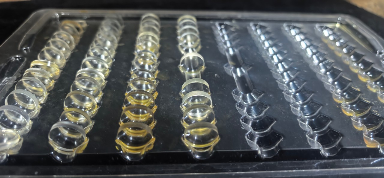
The fourth trap is "forcibly joining dissimilar materials." Coating inorganic films (e.g., ITO conductive layers) onto plastics (PET, PC), or oxides onto metals, without an interlayer, results in mismatched thermal expansion and incompatible chemical bonding – the interface becomes a ticking time bomb. Typical symptom: the coating barely passes cross‑cut testing right after deposition, but after thermal cycling or humidity‑heat aging, it delaminates extensively. Such problems are very difficult to detect before shipment, often only surfacing at the customer site. The cost of rework and compensation then far exceeds the original coating cost. The bottom‑line solution is simple: a transition layer must be added between dissimilar materials – for example, a NiCr layer between glass and silver, or a silicon dioxide layer between plastic and ITO. Sacrifice one layer's thickness to save the entire interface.
The fifth trap is "compulsive multifunctionality." Requiring a single coating to simultaneously achieve ultra‑high transmission, anti‑fingerprint, antimicrobial, conductive, and abrasion‑resistant properties – different materials often conflict with each other. For example, applying an anti‑fingerprint layer on top of an AR coating: if the thickness is not well controlled, reflectivity can jump from 0.5% to 2%. Covering a conductive film with a protective layer: if the protective layer is too thick, resistance doubles and touch sensitivity becomes sluggish. Moreover, when a multi‑layer composite coating fails, it is often impossible to identify which interface is at fault, leading to debugging cycles that drag on for months. When designing, learn to subtract: prioritize functions – which are "must‑have" bottom lines and which are "nice‑to‑have" enhancements – and first ensure the reliability of the core functions.
The sixth trap sounds counterintuitive: over‑inspection. When quality standards are set to "zero defects" without distinguishing between critical defects and cosmetic blemishes, a dust particle less than 0.1 mm in diameter, a barely visible color difference, or a gradual thickness variation at the edge can all cause rejection, artificially lowering yield. For example, in an automotive touchscreen project, the team insisted on raising the cross‑cut test standard from 4B to 5B and required 100% inspection. As a result, yield dropped from 92% to 78% – yet 14% of the "failures" were merely slight edge lifting during tape peeling, with full functionality intact. The correct approach is graded control: zero tolerance for functionally critical defects, and reasonable acceptance criteria for cosmetic issues. Do not sacrifice real output for the sake of impressive numbers.
Ultimately, yield is not "produced" in the coating workshop – it is "defined" at the design stage. Ten out of ten yield problems that get cursed the most in mass production were already signed off during design reviews. There is a golden rule in engineering: at the design stage, bring in process engineers and ask three questions about every specification, every layer, and every unusual dimension: How much process window does this requirement leave? Can existing fixtures coat this shape uniformly? Will this combination of functions fight against each other? Only by making yield a front‑loaded design consideration can you avoid the dead end of "forcing high specifications with low yield" after mass production begins.

Change in packaging method: individual packaging for samples vs. stacked packaging for mass production – increased scratch risk
This is one of the most overlooked yet damaging problems during the transition to mass production. Scratches that are almost nonexistent during the sample stage, when products are individually packaged, can become the number‑one killer of yield when products are stacked in mass production. This difference stems from fundamental differences in three aspects between the two packaging methods: contact interface, relative motion, and particle behavior.
With individual packaging, each product is isolated in its own space, and the only contact is a one‑to‑one static interface between the packaging material and the product. In the sample stage, soft materials (such as cleanroom paper, expanded polyethylene, or bubble wrap) are typically used, and operators handle the products with extra care. The products are essentially in a "suspended" protected state during transport and storage. At this point, the only risk of scratching comes from the cleanliness before packaging – as long as the product surface has no particles, the probability of scratching is extremely low.
When switching to stacked packaging for mass production, products are placed directly face‑to‑face in stacks, forming a product‑to‑product‑to‑product multi‑layer contact chain. The front surface of each piece is in close contact with the back surface of the piece above it. Under the combined effects of transport vibration, stacking pressure, and handling operations, micro‑scale relative displacement occurs at the contact interfaces. Even if the amplitude of this fretting motion is extremely small, after dozens of repeated occurrences it is sufficient to leave visible scratches on the coated surface.
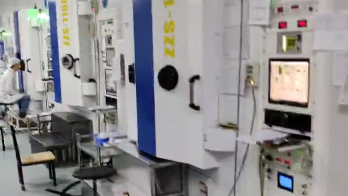
PThe "amplification effect" of particles in stacked packaging is a multiplier of scratch risk. With individual packaging, even if small particles (e.g., environmental dust, coating debris) are present, the lack of relative motion means the particles generally stay in place and do not cause scratches. However, in stacked mass production, the pressure and vibration between products turn particles into "abrasives." A hard particle only 10 µm in diameter (such as glass fragments or detached oxide coating pieces), subjected to tens of kilograms of stacking pressure between two layers of glass and repeatedly rolling during transport vibration, can create a scratch several centimeters long on the coating surface, with sufficient depth to penetrate the AF layer or even damage the AR layer. Even more insidious is that such scratches often appear in "batches" – if a single piece in a stack has edge damage or surface‑attached particles, several adjacent pieces in the same stack may become "contaminated."
The hydrophobic/oleophobic nature of the coating surface ironically becomes an accomplice in stacking. With individual packaging, the high water contact angle (>110°) of an AF anti‑fingerprint layer helps repel contaminants and keep the surface clean. But in stacked packaging, a highly hydrophobic surface means the contact between products is point contact rather than area contact – the actual contact area is small, and the local pressure is extremely high. When the stacking pressure reaches a certain level (typically >50 kg/m²), these high‑stress contact points can cause micro‑plastic deformation or indentations in the coating. More seriously, hydrophobic surfaces easily attract tiny particles from the environment to the contact interface through electrostatic adsorption, further aggravating scratch risk.
Different coating systems have significantly different sensitivity to stacking‑induced scratches, which defines the boundaries for selecting mass‑production packaging solutions. Hard inorganic coatings (e.g., SiO₂, Si₃N₄, DLC) typically have a hardness of 5–30 GPa and good wear resistance, with relatively high tolerance to stacking scratches – although point indentations from particles still need attention. Soft organic coatings (e.g., AF anti‑fingerprint coatings, silicone hard coatings) typically have hardness <3 GPa and are very easily scratched under stacking friction – especially the AF layer, which is only 2–10 nm thick. A single slight relative sliding can wear through the fluorosilane molecular layer, reducing the water contact angle from 110° to below 80°. Metal or transparent conductive coatings (e.g., ITO, silver mesh) face a dual risk: surface scratches may cut the conductive pathways, and even if invisible to the naked eye, can cause touch‑area failure.
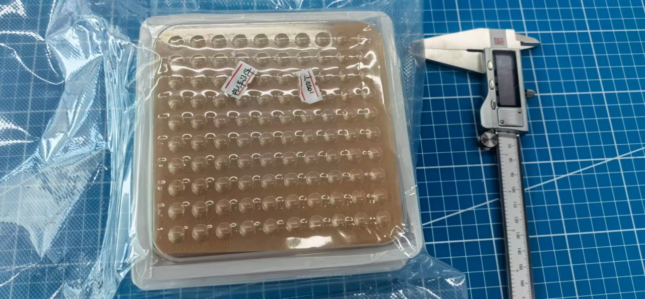
Engineering solutions to the stacking‑scratch problem in mass production require systematic design from three aspects: packaging materials, stacking method, and process control.
Packaging materials: The most critical measure is to insert a buffer isolation layer between every two product layers – for example, cleanroom paper, micro‑foamed PE film, or coated release film. The isolation layer should be thick enough to accommodate small particles (typically >0.1 mm) and made of a material with lower hardness than the coating surface to avoid scratching. For high‑value or high‑precision products, individual interleaving packaging should be used – an isolation material between each product. Although this increases packaging cost, it significantly reduces scratch risk.
Stacking method: Stacking height should be controlled (typically no more than 20–30 pieces) to prevent excessive pressure on the bottom products. Offset stacking or partitioned slots can be used to reduce direct contact area between products.
Process control: The cleanliness of the packaging environment should be raised to a level comparable to the coating workshop (e.g., ISO Class 5–7) to prevent particles from entering the packaging interface. Operators should wear cleanroom gloves and replace them regularly to prevent hand sweat or oil contamination from causing particle adhesion. Vibration and shock during transport should be controlled to prevent relative sliding between stacked products.
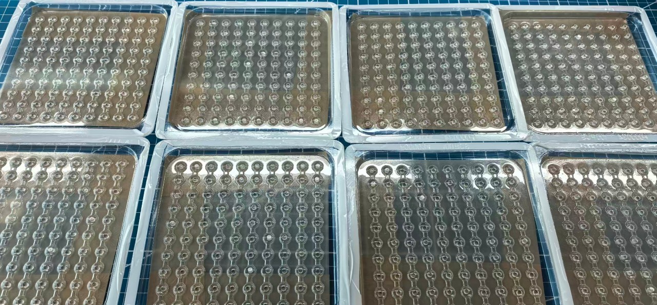
Contact Us
Your feedback fuels our growth, and your questions drive our solutions.
We value your feedback, inquiries, and suggestions. Please feel free to get in touch with us
General inquiries
Please contact us via sales@bo-glass.com, and we will reply to you as soon as possible.
Interested to work with us
Drop your resume at info@bo-glass.com
and we will get back to you shortly.
We uses the contact information you provide to us to contact you about our relevent content, products, and services.